

What is the Identification of the DFM
Design for Printed circuit board manufacturing(DFM) is a process that Organized the PCB designer to design their products in a proper way to fit the manufacturer's production requirement, is like some kind of agreement and Standard.
It can solve some argument between the designer and the manufacturer when it comes to errors of the design due to the destruction of the product.
The function of the DFM enables the manufacturer to examine the design of the products in every expects. Like the dimension, materials, Drill, Holes, Solder mask act. after the inspection, the manufacturer can advise the designer to improve their designing in the first place.
Here we will take some of the basic requirements to be followed in the design of printed circuit boards in electronic products and base on this, you should know that every manufacturer will have some difference due to their capability.
The example of standards is following the below reference.
GB 2036-94 printed circuit terminology
GB 3375-82 terminology of welding
Q / DG 72-2002 PCB design specification
First the Dimension and thickness of Printed Circuit board
1.1: The minimum size of printed board L × W is 80mm × 70mm, and the maximum size L × W is 457mm × 407mm
1.2: The thickness of printed board is generally 0.8-2.0mm.
1.3: outline requirements of printed circuit board
For wave soldering, it is required that the shape should be rectangular. If there is a lack of groove, it should be considered to supplement the lack of groove by means of process panel splicing. For pure SMT board, it is allowed to have a lack of groove, but the size of the lack of groove should be less than 1 / 3 of the length of the side to ensure the smooth transmission of PCB on the chain (as shown in Figure 1)
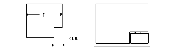
Fiture1 Outline requirements of PCB
2:process side requirements of printed circuit board
In PCB layout, 3-5mm process edge shall be reserved. The so-called process edge is convenient for equipment transmission and clamping during PCB assembly. In this range, it is not allowed to place component pads (except for pads used for whole machine wiring), but wiring can be done. If there are too many components on the printed circuit board, which must not exceed the range of 3mm, add 3mm auxiliary edge on the edge of the board, and the auxiliary edge is opened with V-shaped groove, which can be broken by hand after production.
3:design requirements for mark point of printed circuit board
The reference point is used for automatic alignment of automatic equipment. There are several types of reference points in the visual system. The best reference point mark is a solid circle. The diameter of the reference point mark is generally set to 1mm. PCB reference point and local reference point can be used according to the accuracy requirements. PCB reference point is used for optical positioning of the whole PCB, and local reference point is used for a single device with a large number of pins and a small spacing. The recommended mark points are shown in Figure 2
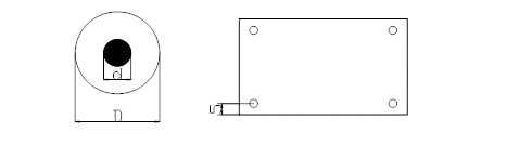
Fiture 2: The design of mark
More about the DFM will be updated for you .
