

High-speed backplane design process
The detailed high-speed backplane design process, in addition to following the IPD (commodity integrated development and design) steps, has a certain uniqueness, which is different from the general hardware configuration PCB control module development process. The key is due to the strong backplane and commodity hardware configuration framework Relevant, in addition to the signal sockets in each hardware configuration control module in the system software, it is also inextricably linked to the design of the entire equipment chassis structure.The design process of the high-speed backplane includes the following design stages:
1. Important technical demonstration of backplane PCB
In addition to the design factors of the PCBA of the switch core backplane, the design of the high-speed backplane must be concerned about the design of the high-speed signal interconnection routing protocol of all system software. The typical high-speed signal routing protocol refers to the following figure:
Therefore, sufficient technical demonstration must be done early, the key include:
①Integrated icSerDes model selection and high-speed signal driver capability verification (analog simulation analysis can also show reference basis, but if the integrated icSerDes can be detected by the Demo board, then testing and certification are more strongly recommended)
②Model selection and certification of high-speed connectors (emphasis on the time and frequency domain index values of the connectors, whether the characteristics of the highest speed signal transmission of the product system can be considered, generally by designing the "connector SI detection board" method)③Model selection of the PCB board (the system software routing protocol includes PCB wiring on both sides of the daughter card and the backplane PCB wiring. The characteristics of the PCB board immediately jeopardize the loss of the routing protocol, and the LowDk / Df board suitable for the specification model must be clearly defined)
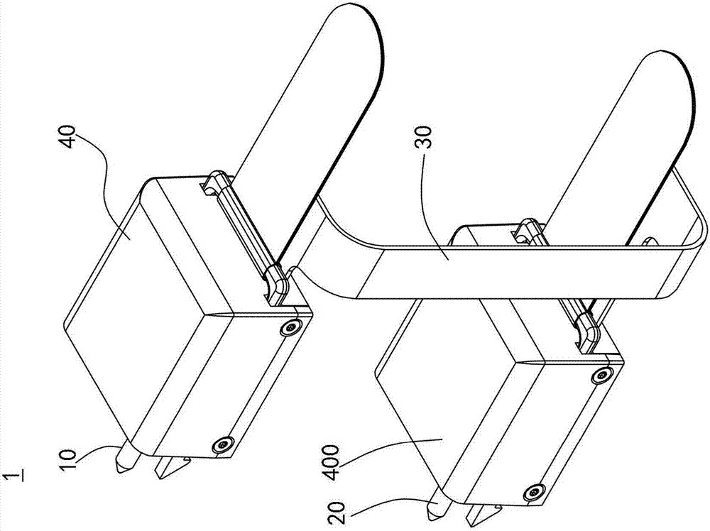
2. Hardware configuration framework design of backplane circuit board
①The function and total number of each double board control module of the system softwareThe overall data information exchange capacity of the system software determines the single-slot data information volume of the business process sub-card in the system software and the total number of business process sub-cards;
The total number of other sub-cards in the system software, such as the total number of key interchange sub-cards, the total number of sub-cards of the main control chip, and the total number of switching power supplies / cooling fan modules of the entire device.
②Model specification and total number of socket connectors for each control module and backplaneAccording to the total number of signals, the actual model selection of the interface connector of each module is decided
③ Frame design related to the design of the whole equipment frameDaughter card slot spacing, daughter card structure-oriented design plan, total power of system software switching power supply, system software heat pipe cooling duct design, etc.
3. Overall design plan
The early important technical demonstration and clear design of hardware configuration framework design completed the plan to generate the backplane overall design plan text file, in addition to the high-speed signal routing protocol pre-simulation simulation analysis.4. PINMAP design
This link has already entered the detailed design and completion of the backplane. Because the backplane has signal sockets in the product system and each hardware configuration sub-control module, all the socket signals must be defined on the socket connector. Established definition, similar to PINMAP with integrated ic pins
On the one hand, the design of the backplane PINMAP must focus on the crosstalk manipulation of high-speed interface signals (for example: the signal must be separated by one GND signal or two GND signals); on the other hand, the completion of the PCBLayout design must be concerned (generally the backplane PCB must be The line is smooth, and the number of superimposed layers on the high-speed backplane is generally higher. If the signal definition is distorted, the number of superimposed layers on the PCB design will increase exponentially)
PCB Circuit schematic designThe circuit schematic design of the backplane is relatively simple, and it can be produced according to the tool software script developed and designed independently, and PINMAP can be immediately converted into the circuit schematic.
5. PCB design
In the early PCB design work, the backplane PCB design is generally completed without too many difficulty factors. The connection can be carried out according to the clear routing standards. The top priority is to ensure the current-carrying work ability of the power supply system of the system software switching power supply.6. UT detection
The backplane UT unit test volume, focusing on the SI characteristics of the backplane high-speed signal security channel, at this time, the connector test board will be used as a test assistant.7. System software integration test
The whole process of system software integration testing will be longer. Because the backplane itself and each hardware configuration sub-control module have sockets, there will be more detection scenarios under different arrangements and combinations, such as: swapping sub-cards and business processes The communication of the daughter card, the communication between the main control chip sub-card and the business process sub-card, and the communication between the main control chip sub-card and the entire device sub-control module.
The detection of the entire equipment of the commodity, such as high and low temperature tests, temperature cycle systems, and credibility, must also be backplane development, design and design staff to participate in the problem of precise positioning reliability testing with each other.