

The pad is the most important basic unit in PCB design.
According to different components and soldering processes, the pads in the printed circuit board can be divided into two types of non-via pads and via pads.
Non-via pads are mainly used for welding surface mount components, and via pads are mainly used for welding pin components.
The choice of pad shape is related to factors such as the shape, size, layout, heat, and force direction of the component. The designer needs to make a selection based on comprehensive consideration.
In most PCB design tools, the system can provide designers with different types of pads such as round pads, rectangular pads, and rectangular pads.
1. Round Pad
In printed circuit boards, circular pads are the most commonly used pads. For via pads, the main dimensions of circular pads are via size and pad size. There is a proportional relationship between pad size and via size. For example, pad size is generally twice the space size. The non-via circular pads are mainly used as test pads, positioning pads, reference pads, etc. The main size is the pad size.
2. Rectangular pad
Rectangular pads include square pads and rectangular pads. The square pad is mainly used to identify the first pin used for mounting components on the printed circuit board. Rectangular pads are mainly used as pin pads for surface mount components. The size of the pad is related to the corresponding pin size of the component, and the pad size of different components is different.
In order to avoid the phenomenon of deviation and tombstone after over-reflow soldering, the pads at both ends of the chip components under over-reflow soldering 0805 and below 0805 should ensure the symmetry of heat dissipation, and the width of the connection between the pad and the printed conductor should not be greater than 0.3 mm (for asymmetrical pads).
3. Octagonal pad
The octagonal pad is relatively rarely used in printed circuit boards. It is mainly set to meet the requirements of wiring and solderability of the printed circuit board.
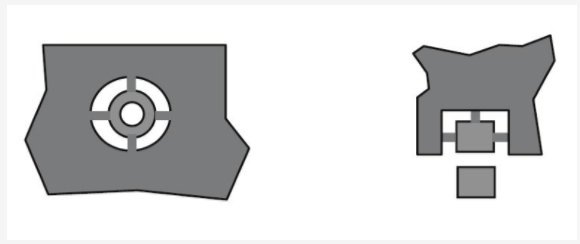
The pad and copper foil are connected in a "meter" shape or a "ten" shape
Figure 1-17 The pad and copper foil are connected in a "meter" or "ten" shape
4. Shaped pad
In the PCB design process, designers can also use some special-shaped pads according to the specific requirements of the design. For example, some pads that generate more heat, have more stress, and have more current can be designed into teardrops.
As shown in Figure 1-17, in order to ensure good tin penetration, the pads of components on large-area copper foil are required to be connected to the pads with thermal tape.
Note: For pads that need to flow a large current of more than 5A, thermal pads cannot be used.
