When we design the product, the PCB board itself will be particularly small, this situation is often unable to meet the PCB
manufacturer's equipment requirements, and resulting in bad production, this time we need to use the Patch design, what
are the forms of the requirements of the patchwork design?
For PCB with long side size less than 50mm, or short side less than 50mm, or size range less than 125×100mm, it is advisable
to use the way of patchment to convert to the ideal size that meets the production requirements for easy assembly. The main
consideration in the splice connection is whether the edges of the splice are neat after separation, whether the separation is
convenient, and whether there is sufficient stiffness in the insertion process
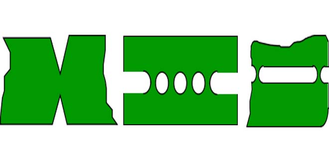
The splice is mainly connected by two-sided V-shaped slot, long slot hole plus round hole and long slot hole, as shown in the figure:

Here are some of Stariver’s requirements for patchwork
|
Items |
Patchwork requirement |
|
|||||||||||||||||||
|
Maximum Size |
OSP |
Thickness≥1.2mm |
720mmX550mm |
|
|||||||||||||||||
|
1.2mm>Thickness≥0.9mm |
650mmX546mm |
|
|||||||||||||||||||
|
0.9mm>Thickness≥0.7mm |
520mmX415mm |
|
|||||||||||||||||||
|
NO OSP |
Thickness≥0.7mm |
720mmX550mm |
|
||||||||||||||||||
|
0.7mm>Thickness≥0.6mm |
520mmX470mm |
|
|||||||||||||||||||
|
0.6mm>Thickness≥0.4mm |
520mmX415mm |
|
|||||||||||||||||||
|
Core LayerCore |
Thickness≤0.4mm |
622mmX520mm |
|
||||||||||||||||||
|
0.4mm<Thickness<1.2mm |
622mmX610mm |
|
|||||||||||||||||||
|
Gold finger |
max 415mmX520mm |
min 132mmX220mm |
|
||||||||||||||||||
|
Plate thickness range: the total plate thickness is generally 0.4-2.5mm; the inner layer core board is the thinnest 0.1mm;(less than 0.4mm and more than 2.5mm plate need to carry on the order review, less than 0.3mm easy plate fold, more than 2.5mm automatic electroplating line plating clip not on) |
|||||||||||||||||||||
|
Maximum number of layers:6 layers; impedance tolerance:/-10%; |
|||||||||||||||||||||
|
Minimum size: OSP70×50 mm; overwashing machine finished product (MIN):35×65 mm; |
|||||||||||||||||||||
|
Plate thickness control tolerance:0.4-0.79±0.08mm;0.8-1.8:±10%;1.8-3.2±0.2mm |
|||||||||||||||||||||
|
|
|
|
|
|
|
|
|
|
|
|
|
|
|
|
|
||||||
|
二、Design requirement |
|||||||||||||||||||||
|
1.0 All typesetting shall be made by the inverted splice. Separate lines and holes shall be arranged into the board |
|||||||||||||||||||||
|
2.0 Selection of material |
|||||||||||||||||||||
|
|
|
Finished copper thickness |
1 oz |
2 oz |
3 oz |
105 um(min) |
all plate electrical thickness 6-8um |
||||||||||||||
|
|
Base board thickness |
|
|||||||||||||||||||
|
|
2 Layers PCB |
1/3 oz |
1 oz |
2 oz |
3 oz |
||||||||||||||||
|
|
Multy layer PCB |
1/3 oz |
1 oz |
2 oz |
3 oz |
||||||||||||||||
|
|
|
|
|
|
|
|
|
|
|
|
|
|
|
|
|
||||||
|
3.0 Goldfinger plates need to put the fingers of the two PCs together against the fingers; the working edge of the gold-plated fingers should be more than 250mm (easy to cross the press machine) |
|||||||||||||||||||||
|
4.0 In order to save cost, usually the double panel design board edge should not be greater than 8.0mm, the four-layer board should not be greater than 10.00mm when making the inner layer, but note that the size of the milling edge should be ≤8.0mm after pressing, so pay attention to the design board edge process hole! |
|||||||||||||||||||||
|
5.0 If the forming method is punching plate, it is necessary to consider that the distance of the die guide column must be more than 3.0mm above the edge of the plate (process edge) to prevent the die guide column baffle from punching the plate normally. |
|||||||||||||||||||||
|
6.0 If the forming mode is punching plate, it is necessary to ensure that the direction of the opening drawing should be consistent with the direction of the punching plate. |
|||||||||||||||||||||
|
7.0 Double-sided and four-layer panels can be used in typesetting to improve plate utilization. |
|||||||||||||||||||||
For different manufacturer,the equipement and capacity are not the same. You can communicate with designers and engineers according to your actual situation


