

1.1 Layout design of components in PCB
1.1.1 Requirements for component layout
a.All use PCB that apply to surface assembly components , should select the same surface assembly design in priority .
b.When using the double-sided surface assembly design, the large package device should be placed on the same side .
c. If there are only the chip-top devices and small-type components in your hybrid PCB design ,those components
should be arranged on the welding surface of the inserted components as far as possible
d.If there is any integrated circuit (PLCC, QFP) with the lead on the four sides in your hybrid assembly PCB, they
should be placed with the plug-in on the same side as possible as you can.
e.Considering the "masking effect" of wave soldering, the installation direction of the components should be desinged
as what was shown in Figure 1.
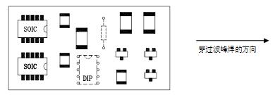
Figure 1 Element orientation on wave soldering substrate
f. Similar components are arranged in the same direction as many as possible, is would be better to placed polar components
on PCB at the same direction as well.
Do not place chip components in the bottom of PLCC and other devices
h.When placing the components in the position where the circuit board is easily bent and deformed, the direction of the components
should avoid the direction which is easy to make the components break or the solder joint break, as shown in figure 16.
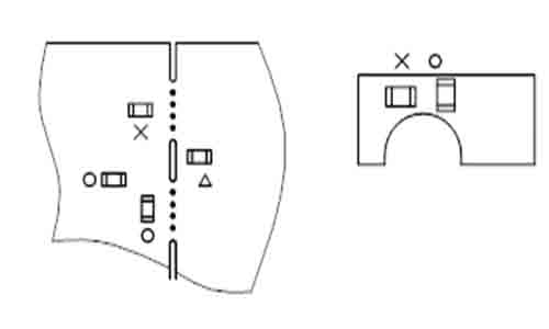
Figure2 Schematic diagram of component location
i. For some devices with large heat capacity and easy to absorb moisture, such as PLCC, BGA should be as scattered as possible on the
PCB layout to avoid the phenomenon of cold welding.
1.2 Requirements for component spacing
a.The spacing between the adjacent surface assembly components (e.g. PLCC, BGA, QFP, etc.) shall not be less than that specified in Fig.17;
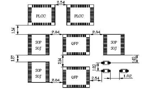
Figure3 Minimum spacing diagram of adjacent surface assembly components (unit mm)
b.For the mixed circuit, the spacing between the through hole inserted components and the surface assembly components shall not be less than the specified in Figure
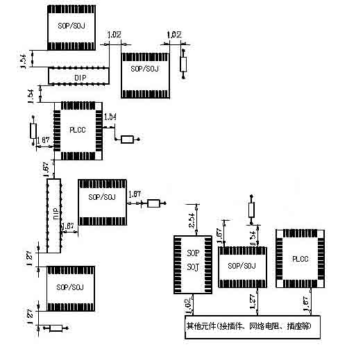
Figure4 Minimum Distance Diagram for Components in Mixed Circuit (Unit mm)
|
|
