

How to make a good design in PCB pads and wire to avoid manufacturing or functional problem, That is the question many of the PCB designer asked, there are some basic rule and tips to share.
1.1.1 line width and distance of printed wire
The line width of printed wire shall be determined according to the wiring density and the current passing through the wire. The commonly used line width is 0.3mm (12mil), 0.2mm (8mil), 0.15mm (6mil), 0.12mm (5MIL). Generally, the thickness of signal line shall be uniform as far as possible to avoid sudden change of thickness and sharp turn. The design of power line, ground wire and large area copper-clad can refer to relevant regulations. Refer to table 7 for pad spacing, line to line spacing, line to pad, line to hole, pad to hole distance during Pad lead out design
Table1 Recommended spacing for several lineweights mm(mil)
|
line width |
0.3(12) |
0.2(8) |
0.15(6) |
0.12(5) |
|||||
|
PCB layer Spcing |
Outer |
Inner |
Outer |
Inner |
Outer |
Inner |
Outer |
Inner |
|
|
Pad Spacing |
0.25 (10) |
0.25 (10) |
0.2 (8) |
0.2 (8) |
0.15 (6) |
0.15 (6) |
0.12 (5) |
0.12 (5) |
|
|
Line to Line |
0.25 (10) |
0.25 (10) |
0.2 (8) |
0.2 (8) |
0.15 (6) |
0.15 (6) |
0.12 (5) |
0.12 (5) |
|
|
Line to Pad |
0.25 (10) |
0.25 (10) |
0.2 (8) |
0.2 (8) |
0.15 (6) |
0.15 (6) |
0.12 (5) |
0.12 (5) |
|
|
Line to Hole |
0.38 (15) |
0.45 (18) |
0.3 (12) |
0.41(16) |
0.18 (7) |
0.33(13) |
0.15 (6) |
0.33(13) |
|
|
Pad to Hole |
0.38 (15) |
0.45 (18) |
0.3 (12) |
0.41(16) |
0.2 (8) |
0.33(13) |
0.18 (7) |
0.33(13) |
|
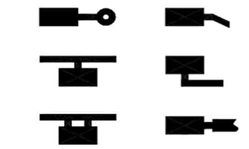
The outgoing line of the pad shall be led out vertically from the middle as precisely as possible, as shown in Figure 19
|
|
|
 |
1.1.2 Design of connection between pad and pad
The wire between adjacent pin pads of the same multi pin component shall be short circuited through outgoing wire, as shown in Figure 16 (a). Generally, the method of direct short-circuit of pad is not adopted, as shown in FIG. 20 (b).
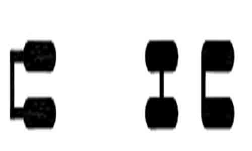
A. recommend B.Not recommend
FIG20 Wiring diagram of pad
1.1.3 Design of connecting wire between pad and through hole
Lead wire connection shall be adopted between the pad and the through hole, and the
distance between the through hole and the pad edge shall be greater than 0.5mm..No through holes are allowed in and on the edge of the surface assembly welding pad, as shown in Figure 21
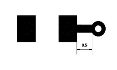 |
Figure 21. wiring diagram of pad and through hole (unit: mm)
