The measurement and the function test of PCB .
Many of the Customers will ask for an outgoing report for their PCB board following with their packages, but do you know how it was made? Today we will introduce the general tools and test methods for the outgoing report to you for a better understanding of this process.
Usually, the outgoing report of PCB includes two main parts: the measurement and the function test :
-
measurement: board thickness, dimension checking, hole diameter, minimum track(Line) width/gap, Surface finish thickness, bow&twist.
-
Function test: microsection, thermal shock test, solderability test, solder mask hardness, and solvent test, the test result should be recorded in the inspection report. Soldermask solvent test.
And the Outgoing report should be made based on the following rules.
1) customer General requirement
2)customer provided Spec
3).EQ;
4).customer FQC inspection standard.
5).factory Lot card
So base on the above information, let's come to the detail one by one.
Bow and Twist
Tooling : flat marble and pin gauge
Method: According to IPC TM650 2.4.22 IPC class 2 Standard: 0.75% for boards with SMT , 1.5% for the boards without SMT
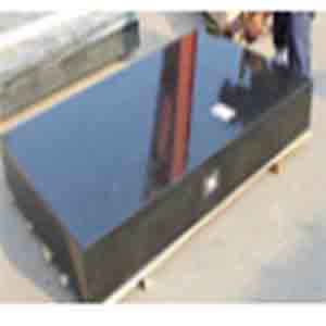
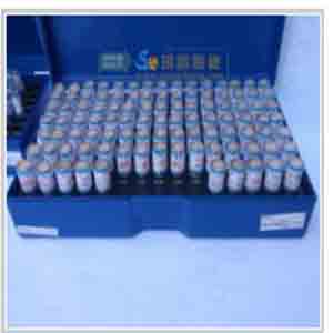
Picture1 : Flat marble Picture2:Pin Gauge
b. Board thickness checking
Tooling: Micrometer or similar board thickness inspection machine
Method:
Measure on the thickest location on both sides, for example, the Hasl board thickness, will need to measure from the surface of Tin pads on the top side to the surface of Tin pads on bottom side. Measure on 4 different locations of the set.
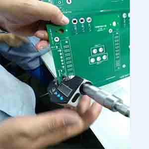
Picture3. Micrometer Inspection
c. Surface finish thickness
Tooling: CMI 900 or Fisher or Similar machine
Method:
Immersion Tin/Gold/silver thickness: measure on the pads close to 1X1MM or 2X2 MM, randomly 5 pads need to be measured on each a set.Hasl Tin thickness: measure 9 points on each panel , All of the 4corners and middle points will be measuredsee below for reference. Select the thinnest point to measure
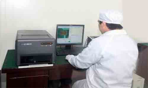
CMI900
d. Track width/gap measurement
Tooling: 100 times magnifier glass or electronic measurement track width/gap checking machine
Method: Check the minimum gap/width according to MI,test standard : width is C in below picture.
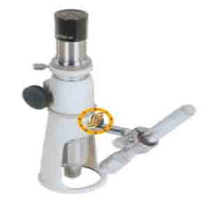
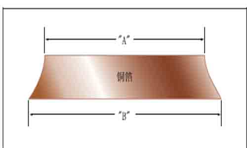
100 times magnifier glass Copper Foil
e. Hole diameter tolerance
Tooling: Pin gauge or automatic hole counter machine
Method by pin gauge:
Measure according to hole tolerance, For example 1.0mm holes with tolerance +/-0.075mm .first use 0.925mm pin gauge to plug into any of the 1.0mm holes, the pin gauge should can go through the holes smoothly without extra push. Then use 1.075mm pin gauge to plug in to any of the 1.0mm holes, the pin gauge should can not plug into the holes. That means holes tolerance is ok.Then use the pin gauge between 0.925mm and 1.075mm to test the 1.0mm holes, when the pin gauge is just fixed in the holes means it's the correct hole diameter, then should record the diameter down and write into the outgoing report.
f. Outline dimension
Tooling: Ruler and 2D element machine
Method & process:
The square or rectangle shape of PCB boards are ok to measure by Ruler, for the un-regular shape boards need to be measured by 2D element machine.The locations which need to be measured in the outgoing report is from the MI mechanical drawing. The tested value should be within the give tolerance in MI.
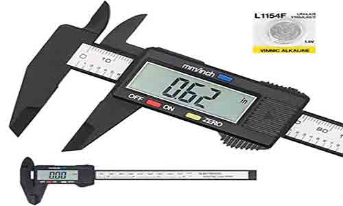
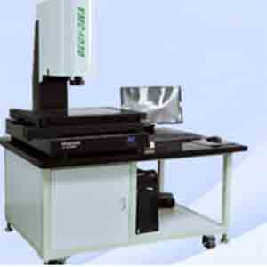
Ruler 2D Element Machine
g. V-cut remain thickness
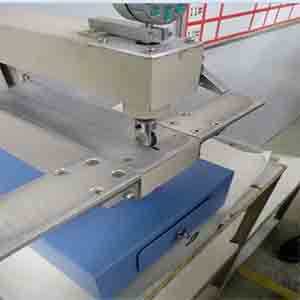
Tooling: Remain thickness tester
Method & process:
One V-cut lane need to test at least 3 locations, one is in the beginning area , one is in the middle , one is in the end area . The measured value should within the range of the MI given tolerance. Funtion Test
Remain Thickness Tester
a. Microsection
Tooling: high times microscope
Method & Process:
Refer to the microsection catalog
b.Thermal shock
Tooling: Solder pot & Stop watch
Method & Process:
cover the board surface with flux, Dip the board into the solder pot with temperature 288+/-5 degrees for 3 times.
Standard :
No soldermask blister, no delamination found.
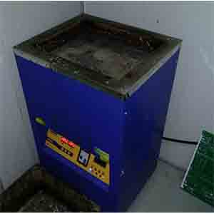
Solder Pot&Stop Watch
c.Solderability test
Tooling: Solder pot & Stop watch
Method & Process:
test condition: Dip test 260+/-5 degrees 3 to 5 seconds .(PB Hasl boards should use solder pot with PB , lead free product should usesolderpot without PB)
Requirement:
All of the surface area should have good wetting and only small pin hole, dewetting and sand area are allowed in the rest of the areas .And these defects should not concentrate in one area.
d. Soldermask hardness test
Test method per IPC-SM-840C 3.5.1 and IPC TM 650 2.4.27.2 . For example 6H hardness.use 6H pencil, pencil touch the soldermask surface closely with angel 45 degrees and make around 6.4mm length writing and there is no scratch into the soldermask surface .
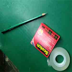
e. Soldermask solvent test
Test method per IPC-SM-840C 3.6.1.1 and IPC TM 650 2.4.27.2 ,
The cured solder mask coating shall not exhibit a degradation in surface characteristics, such as surface roughness, swelling,tackiness, blistering, or color change.
If NG, Record the deviation in the list and report to quality department for verification.
Any if this test and measurement is in good standard, Then the report will be made and send to package department for delivery.


