

With the continuous improvement of human living environment requirements, the environmental problems involved in the PCB production process are particularly prominent. The topic of lead and bromine is the most popular, lead-free and halogen-free will affect the development of PCB in many ways.
Although at present, the change of PCB surface treatment process is not great, it seems to be a relatively distant thing, but it should be noted that long-term slow change will lead to great changes. In the case of more and more environmental protection calls, PCB surface treatment process will definitely change in the future. The basic purpose of surface treatment is to ensure good solderability or electrical properties. As the copper in nature tends to exist in the form of oxide in the air, it is unlikely to remain the original copper for a long time, so other treatments are needed for copper. Although strong copper flux can be used to remove most of the copper oxides in subsequent assembly, the strong flux itself is not easy to remove. Therefore, the industry does not usually use strong flux.
PCB surface treatment
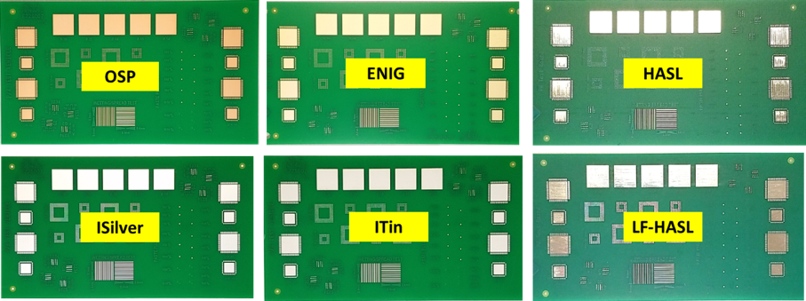
Now there are many PCB surface treatment processes, which are usually five processes, such as hot air leveling, organic coating, electroless nickel plating, gold leaching, immersion silver and tin leaching.
Hot air leveling (HASL)
Hot air leveling, also known as hot air solder leveling (commonly known as tin spray), is coated with molten tin (lead) solder on the PCB surface and heated by compressed air (blowing) to make it form a coating that is resistant to copper oxidation and provides good solderability. Copper tin intermetallic compound is formed at the joint of solder and copper during hot air leveling. PCB should sink in the molten solder when hot air leveling; the air knife blows the liquid solder before the solder solidifies; the air knife can minimize the meniscus of solder on the copper surface and prevent solder bridging.
Organic solderability protectant (OSP)
OSP is a process for printed circuit board (PCB) copper foil surface treatment that meets the RoHS directive requirements. OSP is the abbreviation of Organic Solderability Preservatives. It is translated as organic protective coating, also called copper protection agent. In English, it is also called Preflux. To put it simply, OSP grows on a clean bare copper surface by chemical means.
This film has oxidation resistance, heat shock resistance and moisture resistance to protect the copper surface from further rusting (oxidation or vulcanization, etc.) in the normal environment; however, in the subsequent high temperature welding, this protective film must be easily removed by the flux, so that the exposed clean copper surface can be combined with the molten solder in a very short time to become a solid welding Point.
Full plate nickel plated gold
Nickel plated gold is plated on the surface of PCB conductor with a layer of nickel and then plated with a layer of gold. Nickel plating is mainly to prevent the diffusion of gold and copper. There are two kinds of electroplated nickel gold: soft gold (pure gold, the gold surface does not look bright) and hard gold (the surface is smooth and hard, wear-resistant, containing cobalt and other elements, the gold surface looks bright). Soft gold is mainly used to make gold wire in chip packaging, while hard gold is mainly used for electrical interconnection in non welded areas.
Immersion Gold
The gold deposit is a thick nickel alloy with good electrical properties on the copper surface, which can protect PCB for a long time. Besides, it also has the endurance to the environment that other surface treatment processes do not possess. In addition, gold deposition can also prevent the dissolution of copper, which will be beneficial to lead-free assembly.
Immersion Tin
Since all solder is based on tin at present, the tin layer can match any type of solder. The tin deposition process can form a flat copper tin intermetallic compound, which makes the tin deposition have the same good solderability as the hot air leveling without the headache flatness problem of hot air leveling; the tin deposition plate cannot be stored for too long, and the assembly must be carried out according to the order of tin deposition.
Immersion silver
The silver deposition process is between organic coating and electroless nickel plating / gold deposition. The process is relatively simple and fast. Even exposed to hot, wet and polluting environments, silver still maintains good solderability but will lose its luster. Silver deposition does not have the good physical strength of electroless nickel / gold deposition because there is no nickel under the silver layer.
Chemical nickel palladium
Compared with gold deposition, chemical nickel palladium has a layer of palladium between nickel and gold. Palladium can prevent the corrosion caused by displacement reaction and make full preparation for gold deposition. Gold is tightly covered with palladium, providing a good contact surface.
Hard gold
In order to improve wear resistance of products, increase the number of inserting and pulling and electroplating hard gold.
Gold finger
Usually for some USB port or some orther port will need use gold finger to make sure the quality is stable.
