PCB fabrication is very complicated process, to ensure a good quality board, Multiple structural Inspection technology like Visual Inspection Automated Optical Inspection(AOI),X-ray measurement , Microsection measurement are required.
Here we will introduce how a Microsection exactly works in PCB inspection.
Firstly the Microsection making process
The Steps
1: Punch out Model from the Panel >>2:Fill Resin>>3:Standing 15 to 30 Minutes>>4:Grind with 400# sand paper>>5:Grand with 800#Sand Paper>>6:Grind with 2500# sand Paper>>7:Polish>>8:Micro Etching >>Measurement
Below picture is the process punching out a piece from the Panel

2. Microsection checking equipment & capability & calibration
Capability
50 times : measure the overview board thickness, core thickness
100 times : measure dielectric thickness
200 times : measure copper thickness in the hole and on the surface ,
And measure soldermask thickness, inner layer copper thickness
500 times : used for very precision measurement for verification
3. Microsection used in process discription
PTH backlight: To verify hole wall quality of PTH
Frequency : once per 2 hours
Panel plating : To check copper thickness on the hole wall and on the copper surface Frequency : only do when the via holes are too small, CMI machine can not measure .
Pattern plating : To check copper thickness on the hole wall and on the copper surface
Frequency : only do when the via holes are too small, CMI machine can not measure .
Finished boards : To check copper thickness in the hole and on the copper surface,
check soldermask thickness and other function deviation ,
Frequency : one panel per lot
Due to customer received microsection is only the finished microsection, so below will only talk about the finished board microsection
3:Finished board microsection checking items .
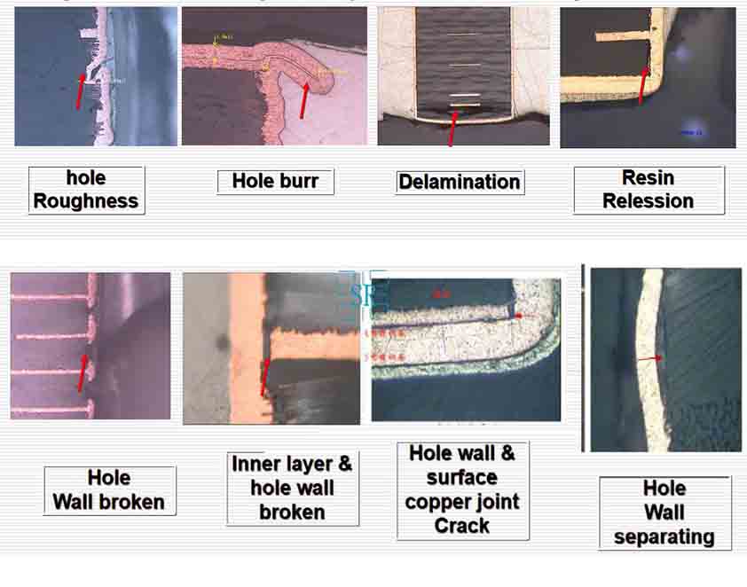
After get microsection, the operator first will check if there is any function problem .
(To simulate more cruel environment , supplier will select some boards and pass thermal shock test with 288 degrees 10 seconds 3 times then make microsections and test these items. But this will not be for every PN just select few boards for process monitor per day)
Below pictures are the sample of major deviation defected pictures.
5. Copper thickness & soldermask thickness measurement .
If there is not any function problem in the microsection , then operator will check Copper thickness & soldermask thickness etc.
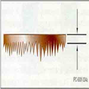
A:Inner layer/outer layer copper thickness, see below picture, If Inner layer or outer layer copper is roughness, need to measure from the middle of the branches
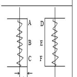
b. Copper thickness in the hole, See below picture , measure A B C D E F six places and for average. And there is also minimum copper thickness requirement for any single point (IPC class2 asked 18um min for single point and 20um min for average )
5.1 Copper thickness & soldermask thickness measurement .
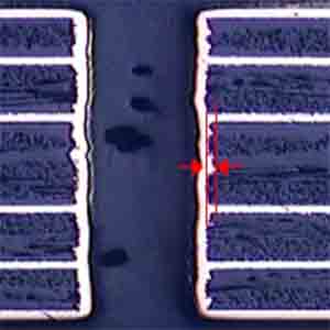
Roughness in the hole measurement
See below picture : measure from the farthest copper residue to the smoothed hole wall area .
Soldermask thickness measurement
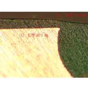
Measure from outer layer to the top of soldermask layer , it’s copper thickness on the surface , corner of the soldermask thickness also need to be measured and normally need to be minimum 5um
Relative Articles :
The measurement and funtional test of PCB


